全国统一电话
全国统一电话
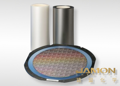
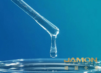
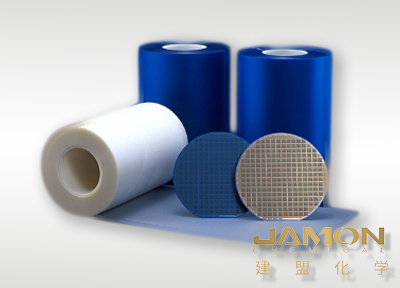
背面研磨胶带介绍
Backside Grinding Tape is used to protect the wafer surface during wafer back grinding after the device is formed on the wafer and the wafer passes tests.
背面研磨胶带用于在晶圆上形成器件且晶圆通过测试后,在晶圆背面研磨期间保护晶圆表面。
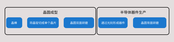
Back grinding occur only on the back side of the wafer, during this process chemically contaminated parts of the wafer removed and thickness of the chip reduced.
The thickness of the wafer defines the size of the finial package, which in turn, is useful to reduce resistance of the chip and power consumption.
背面研磨仅发生在晶圆的背面,在此过程中,晶圆的化学污染部分被去除,芯片的厚度减小。晶圆的厚度决定了最终封装的尺寸,这反过来又有助于降低芯片的电阻和功耗。
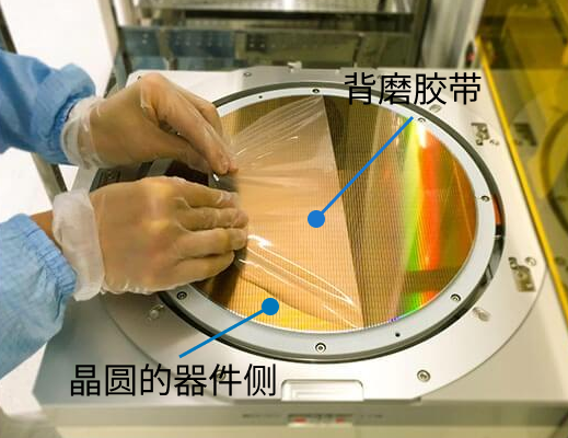
Back grinding tapes, attached on the circuit surface, wafer front side. It prevents damages to the circuit and pollutions to the wafer surface and improves the grinding accuracy of the wafer.
Especially,it can perfectly protect the wafer pattern surface and the chip during the manufacturing process with its excellent physical and chemical properties。
On the other hand, thin wafers can be easily band or get broken, which makes their handling very difficult。
背面研磨胶带,贴在电路表面,晶圆正面。防止电路损坏和晶片表面污染,提高晶片的研磨精度。尤其是其优异的物理化学性能,可以在制造过程中完美保护晶圆图案表面和芯片。另一方面,薄晶圆很容易弯曲或断裂,这使得它们的处理非常困难。
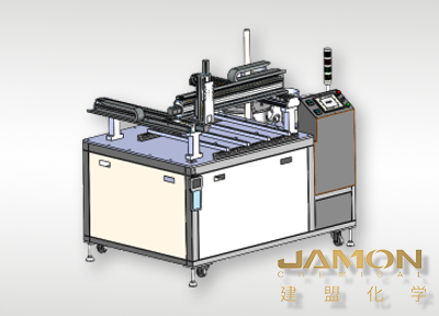
Back grinding process
背面研磨过程
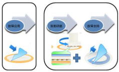
It is typically divided in 3 steps, taping, grinding and tape removing.
1)Tape mounting to the front side of the wafer. During this step it is necessary that there is no bubbles or air traps.
2)Back grinding process. Can be performed in 3 steps, coarse, fine grinding, and Chemical Mechanical Planarization (CMP) or supper fine grinding.
3)The last process is the tape peeling, wherein BG tape is removed from the wafer front side.
Typically, UV and non-UV tape removing. After peeing of the tape there should be no residue left on the wafer.
它通常分为3个步骤,胶带、研磨和胶带去除。
1)胶带安装到晶圆的正面。在此步骤中,必须没有气泡或空气陷阱。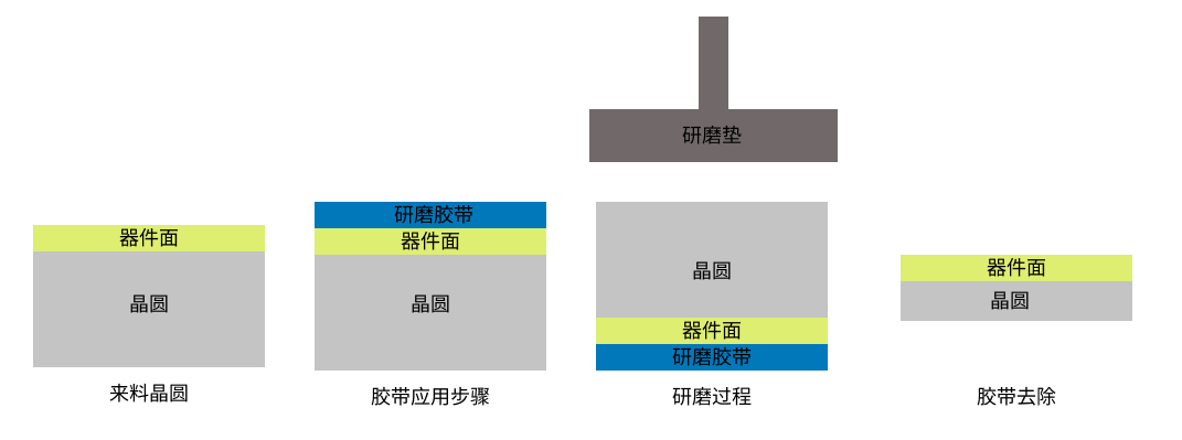
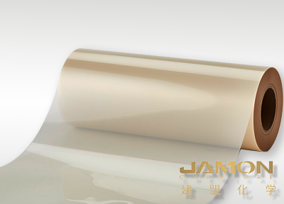
Tape structure
胶带结构
Tape is usually 3 layers, but some tapes have more layers depending on surface construction of wafer/substrate and process requirements.
胶带通常为3层,但根据晶圆/基板的表面结构和工艺要求,有些胶带的层数更多。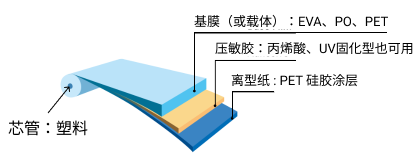
所需功能
| 结构 | 功能 | 目的 |
| 基膜载体
| 垫子 | 防止研磨影响 |
|
| 准确的厚度 | 研磨后晶圆厚度均匀 |
|
| 无缺陷(ex. fisheye) | 防止损坏晶圆 |
| 粘合剂
| 低污染 | 低从粘合剂转移 |
|
| 轻度剥离 | 容易从易碎的晶圆上剥离 |
|
| 准确的厚度 | 研磨后晶圆厚度均匀 |
| 衬垫
| 保护粘合剂 | 保持粘合剂清洁。 防止灰尘或污染 |
|
| 粘合剂平整度 | 粘合剂面平整度 |
Tape types
胶带类型
There is major two classification of Back Grinding Tapes, UV Type, Non-UV Type.
To Non-UV belongs wafer that can be directly peeled off, or adhesive strength can be reduced at elevated temperatures and then peeled off.
UV tapes adhesive strength is drastically reduced after ultraviolet irradiation, then tape can be easily peeled off. There is no or minimum adhesive residue left on the wafer surface, there is no cleaning step is necessary after application of UV tapes. Higher initial adhesive strength prevents forming of the bubbles, and low adhesive strength after UV irradiation will not induce high stresses on the wafer, this is necessary。


 扫描二维码 关注微信