In semiconductor news, there are always mentions of fabs marked by size, such as 8-inch or 12-inch fabs. However, what is the so-called wafer? What part does 8-inch mean? How difficult is it to produce large-sized wafers? The following Dongguan Jianmeng Chemical will gradually introduce what is the most important foundation of semiconductors-"wafer".
1. What is a wafer
Wafer is the basis for manufacturing various computer chips. We can compare chip manufacturing to building a house with Lego bricks, and by stacking layer by layer, we can complete our desired shape (that is, all kinds of chips). However, if there is no good foundation, the built house will be crooked, which is not what you want. In order to make a perfect house, you need a stable substrate. For chip manufacturing, this substrate is the wafer that will be described next.
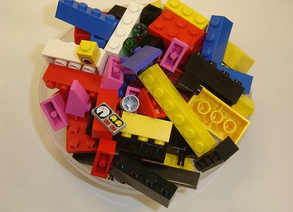
Recall first that when I was a child playing with Lego bricks, the surface of the bricks will have a small round protrusion. With this structure, we can stack the two bricks together firmly without using glue. In chip manufacturing, in a similar way, the atoms added later and the substrate are fixed together. Therefore, we need to find a substrate with a neat surface to meet the conditions required for subsequent manufacturing. Among solid materials, there is a special crystal structure-monocrystalline (Monocrystalline). It has the characteristics that atoms are arranged closely one after another, and can form a flat atomic surface layer. Therefore, the use of single crystals as wafers can meet the above requirements. However, how to produce such a material, there are two main steps, namely purification and crystal pulling, after which such a material can be completed.
2、How to manufacture single crystal wafers
The purification is divided into two stages. The first step is metallurgical purification. This process is mainly to add carbon and convert the silicon oxide into silicon with a purity of more than 98% by redox. Most metals are refined, such as metals such as iron or copper, and metals of sufficient purity are obtained in this way. However, 98% is still not enough for chip manufacturing and still needs further improvement. Therefore, the Siemens process (Siemensprocess) will be used for purification, so that the high-purity polysilicon required for the semiconductor process will be obtained.
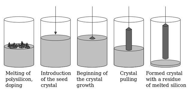
Then, there is the step of pulling the crystal. First, the high-purity polysilicon obtained above is melted to form liquid silicon. After that, the single crystal silicon seed is brought into contact with the liquid surface, and slowly pulled up while rotating. As for why single crystal silicon is needed, it is because the arrangement of silicon atoms is similar to that of people lining up, and it will need to take the lead to let later people arrange it correctly. Silicon is an important heading, so that later atoms know how to line up. Finally, after the silicon atoms leaving the liquid surface solidify, the neatly arranged single crystal silicon pillars are completed.
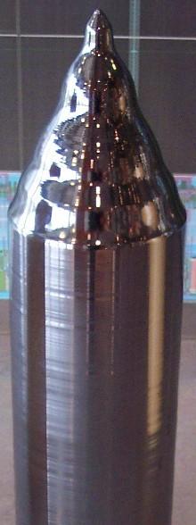
3、Monocrystalline silicon pillar (Souse: Wikipedia)
However, what does 8-inch and 12-inch stand for? In fact, it refers to the crystal column, which is the diameter of the part that looks like a pencil barrel in the picture above. As for the difficulty of manufacturing large-size wafers? As mentioned earlier, the process of making the crystal column is like making marshmallows, forming while rotating. If you have made marshmallows, you should know that it is quite difficult to make large and solid marshmallows. The process of pulling crystals is the same. The speed of rotation and the temperature control will affect the quality of the crystal column. Therefore, the larger the size, the higher the speed and temperature requirements of the crystal pulling, so it is more difficult to make high-quality 12-inch wafers than 8-inch wafers.
However, a whole piece of silicon pillar cannot be used as a substrate for chip manufacturing. In order to produce a piece of silicon wafer, a silicon knife is then required to cut the silicon pillar laterally into a wafer. The wafer can then be polished to form a chip Manufacturing the required silicon wafers. After so many steps, the manufacture of chip substrates is completed.




 Scan QR code Follow WeChat


